
Electronics are changing into costlier for each producers and customers. Why? The reply lies within the fascinating world of semiconductor testing.
An in-depth take a look at the making of those advanced gadgets will provide the justification you want for his or her excessive worth. By comprehending the intricate course of, you’ll really feel extra comfy the following time you’re buying chips for a tool.
Moderately than questioning the worth, you’ll see it as an funding in a masterpiece of know-how. Hold studying to know why your gadgets are value each penny.
Understanding Semiconductor Testing
You could typically marvel the place the brains of your smartphone, pc, or every other digital gadget come from. They’re born from tiny slices of silicon referred to as semiconductors.
Silicon is innocent and plentiful. It’s discovered within the sand.
When thinly sliced into wafers and injected with particular impurities, silicon turns into the constructing block for chips. That features telephone chips, pc chips, and every other built-in circuit.
To make sure the whole lot works completely, every semiconductor ensuing from a wafer has to bear thorough testing. Governments impose sure rules to make sure security, high quality, and efficiency. The regulation of semiconductor testing can differ from nation to nation.
The Beginning Level: Wafers
Your journey begins proper from the harvesting of silicon, the place it will get processed into skinny, round wafers. These wafers are then imprinted with an intricate circuit design that may later develop into the chips that energy your electronics. However earlier than that, they bear wafer testing.
Wafers aren’t freed from defects. Flaws may be something from small cracks to contamination from mud or undesirable particles. Eliminating flawed wafers at an early stage is crucial to keep away from losing assets in subsequent steps.
Most cellphone and pc producers don’t create the wafers themselves. They organize them from producers like silybwafers.com/.
Take a look at Gear within the Manufacturing Course of
Throughout wafer testing, a prober takes photos of potential defects. A wafer prober is a complicated machine that holds the wafer and permits for semiconductor testing of the circuits traced on it.
Along with imaging, probers can perform electrical assessments. The machine probes every circuit hub on the wafer utilizing a set of microscopic needles. When energy is utilized, the prober generates a complete report about every circuit’s performance.
Take a look at Substrates
Take a look at substrates assess crucial parameters resembling movie thickness, etch charges, and sample uniformity. By mimicking the traits of manufacturing wafers, these substrates function a managed atmosphere. Engineers can use them to detect and rectify deviations.
In a course of known as wafer stage reliability (WLR) testing, the wafer is pressured to measure the degradation it causes. This stress could cause the construction to fail in sure circumstances, indicating defects.
Defect Detection Methods
Numerous methods, resembling optical inspection, electron microscopy, scanning acoustic microscopy, and X-ray inspection, provide help to spot pesky defects.
Optical inspection makes use of a high-resolution digital camera for recognizing surface-level defects. It may well embody UV mild, high-powered lenses for zooming actions, and particular algorithms to course of photos taken by high-resolution cameras.
Electron Microscopy
Electron microscopy supplies a deeper look, trying to find any abnormalities contained in the chip itself. Transmission electron microscopy (TEM) is extensively used on this context.
TEM operates by transmitting a beam of electrons via a skinny specimen. The interplay of those electrons with the pattern creates a picture that may show atomic-level particulars. This high-resolution imaging is crucial for observing any potential defects inside the layers of a semiconductor chip.
Acoustic Microscopy
Scanning acoustic microscopy (SAM) makes use of ultrasound know-how to seek for hidden flaws not seen to the bare eye. It is a non-destructive method for fault detection and high quality management.
SAM operates by emitting ultrasound waves at a particular frequency and specializing in the specimen. The sound waves journey via the pattern and replicate once they meet a boundary or defect.
A detector picks up the mirrored waves. Information from these reflections builds a picture of the inside construction of the pattern.
X-Ray Inspection
X-ray inspection works on the precept of X-ray radiography. An X-ray supply emits radiation via the element being inspected. Totally different supplies soak up totally different quantities of radiation primarily based on their thickness.
The denser and thicker the fabric, the much less radiation passes via. These areas seem darker within the picture. Equally, lower-density supplies soak up much less radiation and present up lighter on the X-ray picture.
The detected X-ray picture on the different finish illustrates the inner construction of the half. The important thing utility of this inspection is detecting voids (empty areas) and cracks.
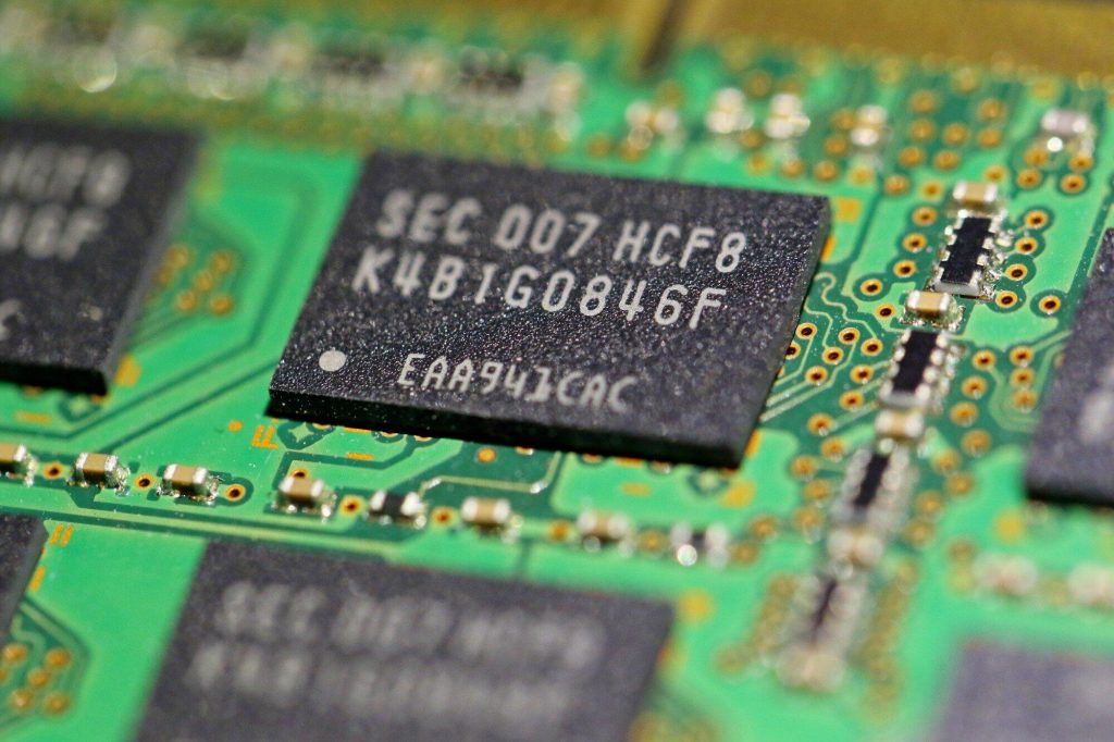
From Wafer to Semiconductor
The wafer is minimize into particular person chips, a course of referred to as dicing. Every chip could comprise quite a few similar circuits, which is able to every perform as an unbiased semiconductor system.
Semiconductor Testing Course of
The semiconductor testing course of is the ultimate gate earlier than coming into the market. After the wafers bear many manufacturing levels, the ensuing chips are as you see them proper earlier than being put in into the one you love devices.
In practical testing, every chip goes via an electrical check that challenges it to behave as designed. Stress testing simulates harsh environments to see if the chip can deal with them. Then, there’s the burn-in check, which sends a steady high-voltage surge to verify whether or not the chip can final for a very long time.
The mixture of all these assessments ensures that solely the most effective semiconductors make their option to the gadgets you love. Any chip failing these assessments is discarded to take care of high-quality requirements.
You may have reached the top of a semiconductor’s journey. Keep in mind that each system you utilize, from a small digital watch to a fancy spacecraft, is a product of this journey.
Boosting Machine Effectivity
Semiconductor testing is essential for guaranteeing the chips in your gadgets act as meant. Wafers, the inspiration of chips, bear intensive inspections all through their transformation into semiconductors. Procedures like optical inspection, electron microscopy, acoustic microscopy, and X-ray inspection guarantee each chip is flawless.
If you wish to elevate the web visibility of your gadgets powered by these meticulously examined semiconductors, dive into our weblog. Right here, you may discover confirmed search engine optimisation practices to boost your product’s on-line presence.